Hello. My name is Kaneko, a second-year master’s student.
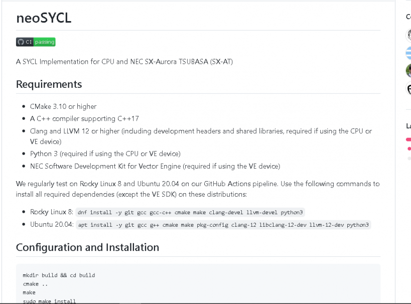
Just a few days ago, “neoSYCL”, an original SYCL implementation developed in this laboratory, was released!
SYCL is a standard developed by the Khronos Group for writing code for heterogeneous architectures.
There are several implementations of SYCL, as described here.
Among them, neoSYCL is the only implementation that supports CPU and NEC’s SX-Aurora TSUBASA (SX-AT) as a processor.
With neoSYCL, processing in heterogeneous systems containing SX-ATs can be written in a single-source program using standard C++.
Please check the neoSYCL page on GitHub for more information.
In addition to SX-AT, my research has also created an extension library to support Intel Field Programmable Gate Array (FPGA), which I plan to research and implement so that it can be published on GitHub.