HOT CHIPS is one of the semiconductor industry’s leading conferences on high-performance microprocessors and related integrated circuits. This year, the latest technologies and products were introduced and presented by engineers and chip designers from famous corporations and national laboratories. The conference was held virtually from August 22nd to 24th.
It had several sessions including CPUs, data processors, machine learning platforms, and etc. There were many innovations and technical improvements introduced in high-quality presentations.
This year, several top-level corporations brought their new CPUs. Here, I am going to share some topics I am interested in and my impressions.
1. Intel Alder Lake
Alder Lake is the newest generation of Intel Core processors. The core design is totally different from the past. It uses two different cores with different architectures, P-core and E-core, to achieve the performance hybrid.
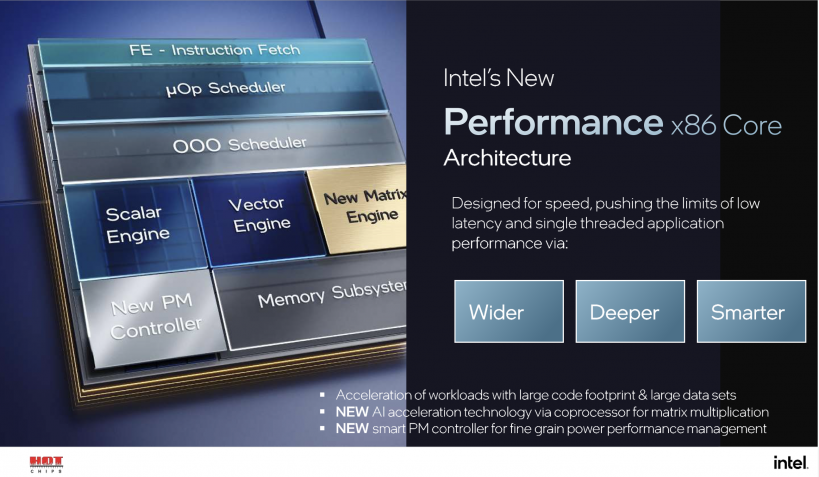
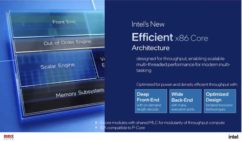
Fig.1 P Core and E Core (source: Intel)
P-core delivers higher performance on single and lightly threaded scalable applications, while E-core provides better throughput on multi-threaded applications. For the scheduling, Intel uses the Thread Director to put the right workload on the right core at the right time. Based on the IPC differences between P-core and E-core, applications are classified into 4 classes. The information on energy efficiency and performance is periodically written into the EHFI table. Then the OS scheduler selects the best core allocation. The Thread Direct architecture is shown as follows.
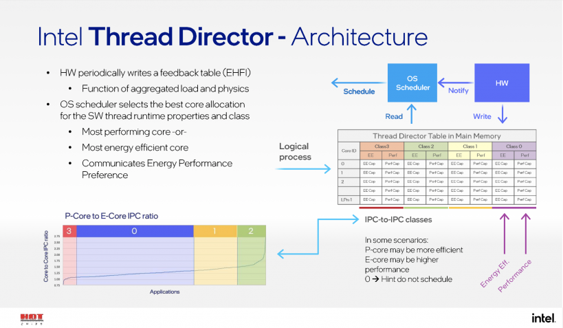
Fig.2 Thread Director (source: Intel)
2. AMD Zen3
Compared to Zen2, the new generation achieves 19% IPC improvement, which is awesome. The figure shows major changes in Zen3.
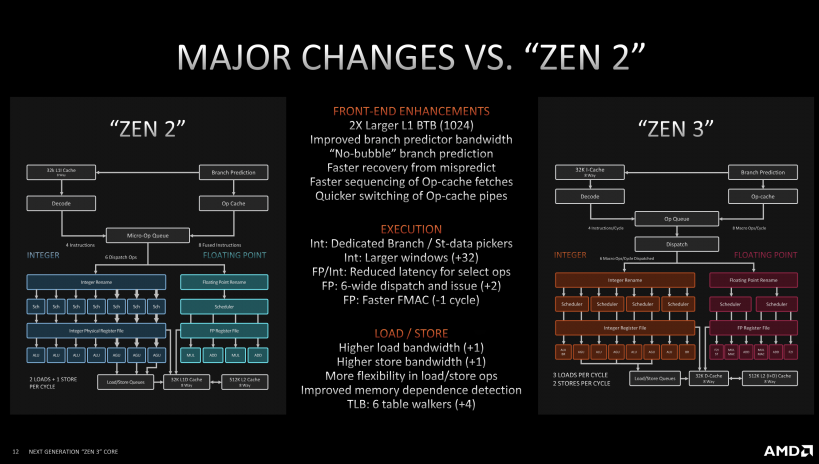
Fig.3 Comparison between Zen3 and Zen2 (source: AMD)
The most interesting part for me is the Zen3 cache hierarchy. Although the total size of the L3 is not changed, the direct accessibility per core becomes twice, which brings the reduction in effective memory latency. The outstanding misses of L2 and L3 are also amazing. Besides, their 3D V-cache technology makes the L3 192MB, which is a surprising capacity.
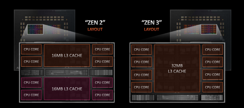
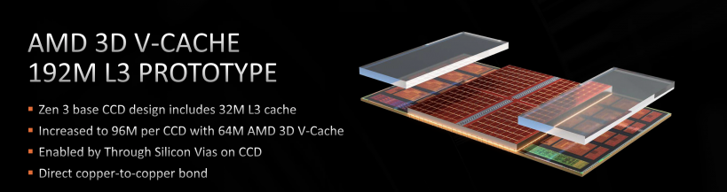
Fig.4 Zen3 Cache Hierarchy and 3D V-Cache (source: AMD)
3. IBM Telum
The new IBM Z system is quite different from Z15, especially the cache hierarchy. Each core has a private 32MB L2 cache, which is 8 times larger than the L2 cache in Z15. However, in Telum, there are no physical L3 and L4 caches, instead, IBM uses L2 to generate virtual L3 and L4 caches. This inspiring design greatly saves chip areas and latencies of L3 and L4, while still remains their functions, and further improves cache size per core. With such implementation, the system can achieve over 40% per socket performance growth.
Fig.5 IBM Telum Cache Hierarchy (source: IBM)
4. Intel Xeon Sapphire Rapids
Recently, modular architecture has become popular in processor design. This is because a smaller die size can bring better yield in the chip fabrication. Thus, Sapphire Rapids uses EMIB technology to achieve a multi-tile design. The acceleration engine in each tile is one important part. It includes data streaming, quick assist technology, and dynamic load balancer, and supports common-mode tasks offload.
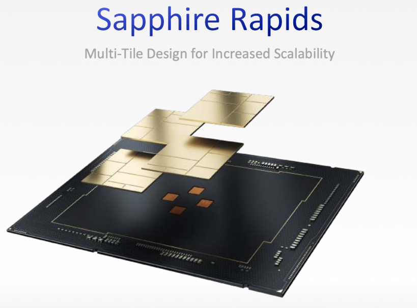
Fig.6 Sapphire Rapids (source: Intel)
In addition, the shared LLC is also increased this time, and the HBM with 2 modes (flat or caching) are mentioned.
There are still many brilliant presentations that I cannot introduce all. For example, Samsung’s HBM2-PIM, the chiplet and 3D packaging, and etc. From this conference, I have learned a great number of inspiring ideas and technologies. I am impressed by their creations and efforts in achieving improvements. These new architectures and ideas show me popular trends in chip design fields and will help a lot for my own research.